🔒 Strict IP Protection & Data Security✈️ AS9100 & IATF 16949 Standards⚡ 100% Manufactured in South Korea · Express Delivery
Manufacturing 24/7 in Korea · Now accepting 2026 orders

Korea's Quick-Turn PCB & PCBA Partner for Global Hardware Teams

From PCB fabrication to component sourcing, SMT assembly, inspection, and global delivery — one accountable manufacturing partner in South Korea.

  • PCB Fabrication
  • SMT / IMT Assembly
  • Component Sourcing
  • Global Shipping

Our Engineering Commitment

DHL Express / FedEx / UPSISO 9001 · AS9100D · RoHS Compliant
450+
Engineers & Production Specialists (Korean network)
6 Lines
Fully Automated SMT Lines
Class 3
High-Reliability IPC Standard
1.4M/day
SMT Placement Capacity · 3D X-Ray & CT

Get a PCB & PCBA Quote

Send us what you have. Our engineers will help complete the manufacturing data package.

Live

Recommended files

PCB Fabrication
Gerber · ODB++ · IPC-2581 · NC Drill · Fabrication Drawing
PCB Assembly
Gerber/ODB++ · BOM · Pick & Place (Centroid) · Assembly Drawing · Schematic (optional)

※ Required: Please click the process(es) you need (multi-select)

All design files are encrypted during transfer and strictly protected under robust IP security protocols.

Detailed DFM feedback is provided after receiving sufficient manufacturing data.

DFM Review: 1–3 Business Days. Send your schematic or drawing; our engineers will advise on stack-up, fabrication data, and DFM requirements.

Encrypted & Confidential
DFM Review: 1–3 Business Days
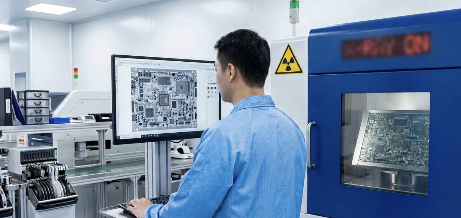
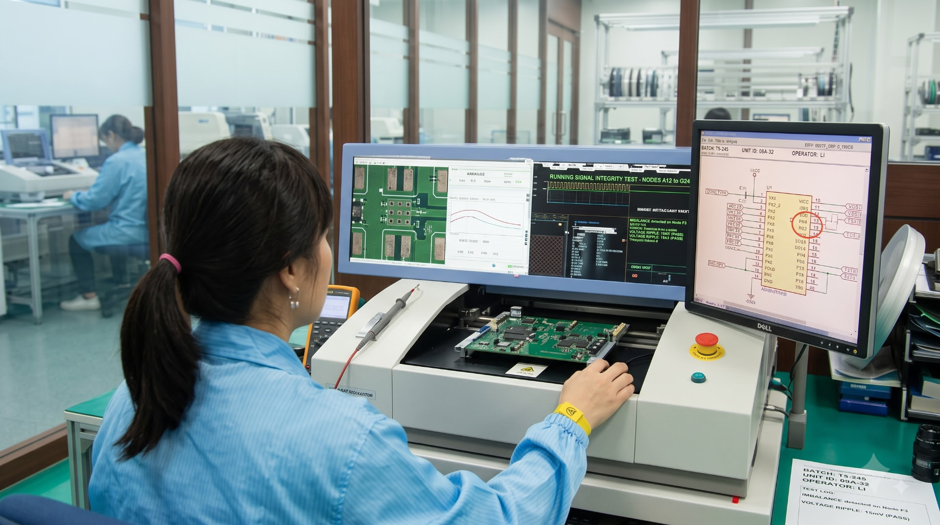
SPI · AOI · 3D X-Ray · E-Test

Design in. PCBA out. Made in Korea. — PCB fabrication, component sourcing, SMT assembly and inspection managed through one accountable partner.

Predictable Workflow

From Design Files to Delivered PCBA

Select a step to see exactly what happens and what you receive.

01. Upload

Send Gerber/ODB++, BOM, and Pick & Place data — or just a schematic. Files are encrypted in transit and handled confidentially, shared only with the assigned engineers.

SMT / PCBA

SMT Assembly Capabilities

High-precision SMT for prototype, NPI and production.

Component Size
0402 standard · 0201 capability available
Packages Supported
BGA, QFN, LGA, fine-pitch components
Assembly Types
SMT + IMT mixed assembly · Lead-free & RoHS compliant
SMT Infrastructure
6 fully automated SMT lines (up to 1.4M placements/day)
Quality & Inspection
SPI, AOI, 3D X-Ray / CT inspection, ESD-controlled production

Component Sourcing

One BOM. One Accountable Supply Chain.

Choose the sourcing model that fits your program — we manage the rest.

Turnkey

Complete component sourcing + PCB fabrication + assembly under one purchase order.

Consigned

You supply all components; we handle kitting verification, fabrication, and assembly.

Mixed

Customer-supplied critical parts combined with team-sourced commodity components.

Component management included

  • MPN verification
  • Lead-time check
  • Authorized distributor sourcing
  • EOL / obsolete review
  • Alternative part review

No component substitution without customer approval.

PCB Fabrication

Advanced PCB Fabrication

From quick-turn prototypes to high-reliability multilayers.

Product Scope & Capabilities

PCB TypeStandard SpecsAdvanced / Special SpecsKey Features
Heavy Oz2–8L10–18L3–10oz Copper Power Supply Board & Bus Bar
Metal Base1–2L (Al/Cu base)4–12LMetal Plate High Heat Dissipation (Heat-sink)
BVH (Blind/Buried Via)4–12L14–24LBlind Via Hole & Buried Via Hole
HDI6–8L10–16LHigh-Technology Multilayer PCB
Flex-Rigid4–8L10–22LHigh-Layer Flex-Rigid / HDI Flex-Rigid
High-Count Multilayer4–20L22–42LHigh-Layer MLB & Probe Cards
Hybrid~8L10–24LSpecial Materials (Rogers, Taconic, Nelco, Isola, PI)

Technical Design Rules & Engineering Limits

ParameterStandardNormally availableAdvancedAvailable by engineering reviewMaximumProject-specific / factory confirmation
Layer Count2–20L22–32L34–42L
Board Thickness0.4–3.2 mm (16–126 mils)4.8 mm (190 mils)Max 6.0 mm (240 mils)
Min Line Width / Space0.1 mm (4 mils)0.075 mm (3 mils)0.05 mm (2 mils)
Min Mechanical Hole Size0.25 mm (10 mils)0.15–0.2 mm (6–8 mils)0.1 mm (4 mils)
Min Laser Hole Size0.10 mm (4 mils)0.08–0.09 mm (3.15–3.54 mils)0.08–0.09 mm (3.15–3.54 mils)
Max Board Size507×607 mm (20×24″)600×800 mm (24×31″)600×800 mm (24×31″)
Impedance Control±10%±7%±7%

Values are typical reference capabilities. Final confirmation is provided after engineering review and DFM analysis.

Quality

DFM Review & Quality Documentation

Know exactly what we check — and exactly what you receive.

Our DFM review includes

  • Trace / space
  • Drill & via structure
  • Copper balance
  • Stack-up
  • Impedance requirements
  • Solder mask
  • Component clearance
  • BGA / QFN considerations
  • BOM availability & EOL risks
  • Panelization & depaneling method
  • Solder paste & stencil considerations
  • Thermal relief & copper pour balance

Available quality documents

  • AOI report
  • 3D X-Ray report
  • Electrical test report
  • First Article Inspection (FAI) report
  • Certificate of Conformance (COC)
  • RoHS / REACH compliance
  • Lot traceability records
Request DFM Review & Inspection Specs

Detailed DFM feedback is provided after receiving sufficient manufacturing data.

Lead Times & Logistics

Predictable Lead Times, Delivered Worldwide

Quote Response
Within 2 business days
DFM Review
1–3 business days
Production & Assembly
Project dependent
Shipping
3–5 business days via express

Global Shipping

DHL Express, FedEx, UPS, or your own freight forwarder — with DAP and DDP Incoterms options.

  • DHL Express
  • FedEx
  • UPS
  • Customer Freight Forwarder
  • DAP / DDP Incoterms

Manufactured in South Korea. Delivered worldwide.

Supply Chain Diversification

Diversify Your PCB & PCBA Supply Chain with Korean Manufacturing

A stable, allied-nation manufacturing base with mature electronics infrastructure, engineering depth, and predictable export logistics.

Manufactured in South Korea

Manufactured in South Korea through a qualified Korean manufacturing network under our engineering supervision and quality control — with full process traceability from fabrication to final inspection.

Geopolitical Stability & Supply Chain Safety

A trusted allied-nation alternative for defense and advanced tech programs, with IP strictly protected under Korean law.

Fast Turnaround & Superior Technical Communication

English-fluent senior engineers answer within hours — no translation layers between your design intent and the production floor.

Technical Excellence

Core Competencies & Technical Excellence

IPC Class 3 & High-Reliability PCBs

Specialized in Defense, Aerospace, and Industrial Grade. Expertise in Rigid-Flex PCBs and Multi-Layer builds from 2 to 42 layers.

Continuous Investment in Next-Gen Infrastructure

Powered by state-of-the-art machinery and automated lines—including pulse plating and ultra-fine pattern tech—ensuring flawless precision for high-density builds.

6 Advanced SMT Assembly Lines

Equipped for components down to 0201 (01005 available upon engineering review) and high-density mounting at up to 1.4 million placement points per day.

Proactive DFM (Design for Manufacturability)

We don't just print your files — we review them and return a defect prevention proposal. DFM Review: 1–3 Business Days.

Quality & Security

State-of-the-Art Smart Factory Network in South Korea

A qualified Korean manufacturing network across Seoul, Incheon, and Ansan — orchestrated as a single production layer.

PCB Assembly

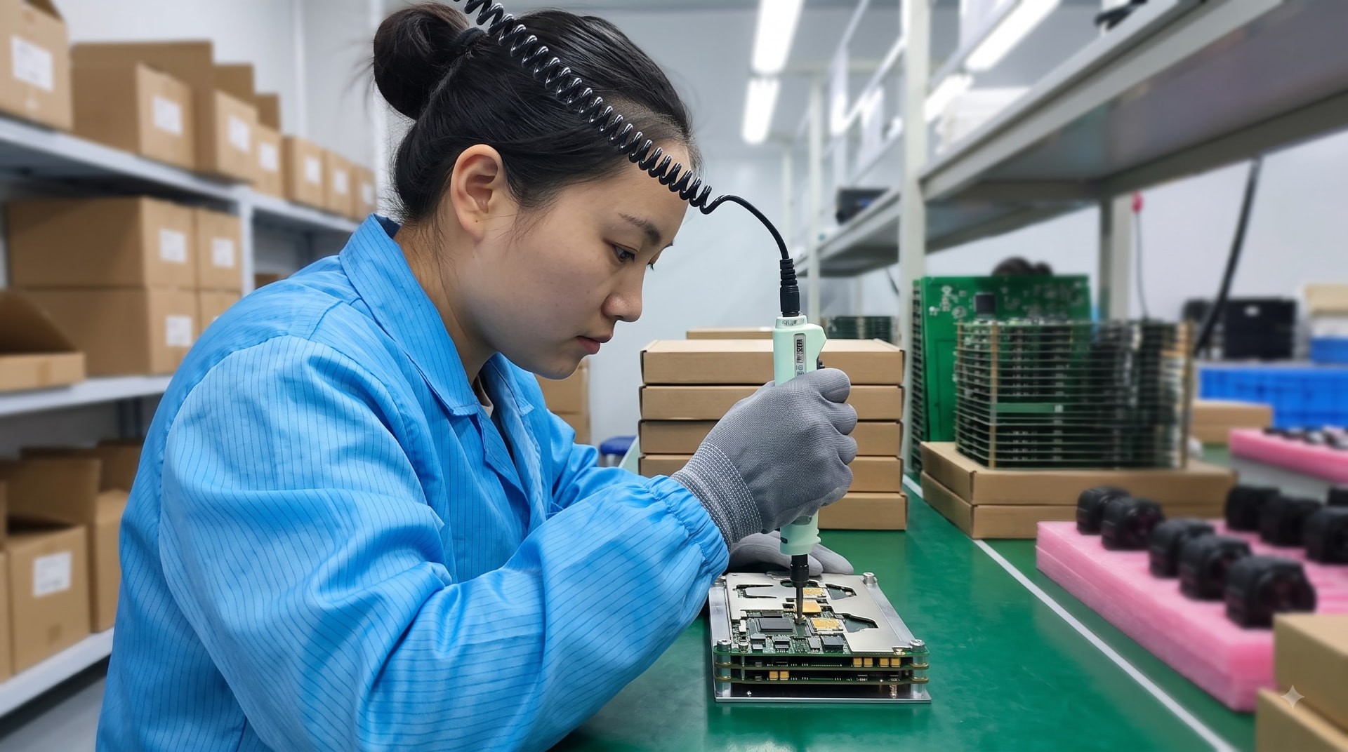
PCB Assembly

Manual PCB assembly with ESD protection and IPC Class 3 workmanship.

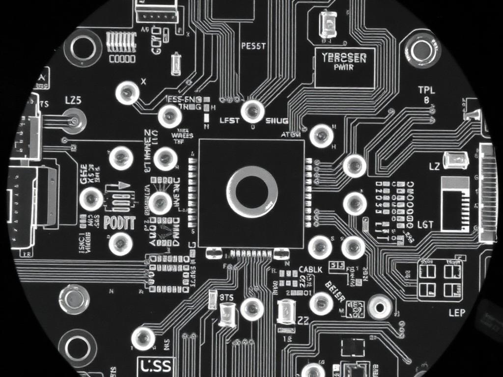
3D X-Ray Inspection

3D X-Ray Inspection

3D X-Ray and CT inspection for BGA, QFN and hidden solder joints — void ratio, bridging, and alignment verification.

AOI Automated Optical Inspection

AOI Automated Optical Inspection

Automated optical inspection for component presence, polarity, offset, and solder fillet quality against IPC acceptance criteria.

Auto-Plating Lines

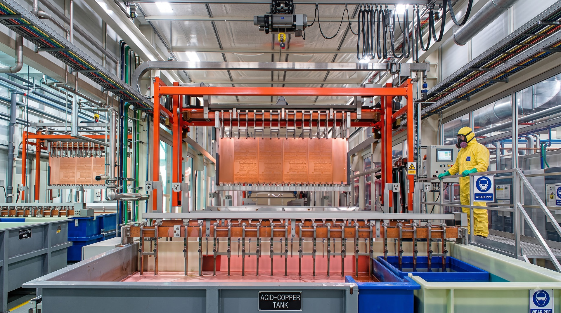
Auto-Plating Lines

Automated acid-copper plating line for uniform deposition across high-density panels, maintaining consistent copper thickness ±5%.

Quality & Compliance

Quality & Compliance

Certifications and standards applied across our qualified Korean manufacturing network.

  • ISO 9001Quality management systemDocumented, audited process control on every order.
  • AS9100DAerospace quality managementTraceability and configuration control for high-reliability programs.
  • IATF 16949Automotive quality managementProcess discipline suited to automotive-grade volume builds.
  • ISO 14001Environmental managementControlled chemical handling and waste management.
  • IPC-A-600Bare board acceptabilityBoards judged against IPC Class 2 or Class 3 criteria as specified.
  • IPC-A-610Assembly acceptabilitySolder joint and workmanship criteria applied to every PCBA.
  • ULMaterial & flammability listingUL-recognized laminates with UL marking available on request.
  • RoHS / REACHSubstance complianceLead-free process with compliance declarations issued per lot.

All production within the NexTurnPCB network is strictly executed in compliance with these international quality standards and IPC workmanship guidelines.

Data Scope

Drawing & Technical Specification Scope

Send what you have. We handle the rest of the data package.

Input

What you send us

  • Schematic
  • Component Layout (Dimension)
  • Gerber Data

Output

What we deliver back

  • Full Artwork
  • Fabrication Drawing
  • Gerber
  • Assembly Drawing

DFM Feedback

Target Turnaround

  • DFM Review: 1–3 Business Days
  • Defect prevention proposal
  • Stack-up & impedance advice

Case Studies

Programs We Manufacture

Anonymized examples of typical builds handled by our Korean manufacturing network.

High-Reliability Multilayer PCB

ChallengeHigh signal integrity & strict IPC Class 3 compliance on a 20-layer board.
SolutionHigh-Tg Tg170+ material selection, precise stackup design & 100% coupon impedance testing.
ResultZero-defect lot delivery with full lot traceability & IPC Class 3 certification.

20 Layer · 1.6 mm · ENIG · Controlled Impedance · IPC Class 3

Fine-Pitch BGA PCBA

ChallengeSolder joint reliability & voiding prevention on 0.4 mm fine-pitch BGAs.
SolutionOptimized stencil design, SPI + 3D X-Ray void analysis & custom reflow profile.
Result< 5% BGA void rate achieved & 100% FAI approval for mass production.

0.4 mm pitch BGA · 1,800 placements · SPI + AOI + 3D X-Ray

Prototype to Production

ChallengeScaling rapid 10 pcs prototype builds to 2,000 pcs/month repeat production without quality drift.
SolutionEarly DFM optimization, frozen BOM management & standardized FAI procedures.
Result100% on-time delivery & seamless ramp-up with zero assembly defect rate.

10 pcs prototype → 2,000 pcs/month · Frozen BOM · FAI documented

Representative process visuals

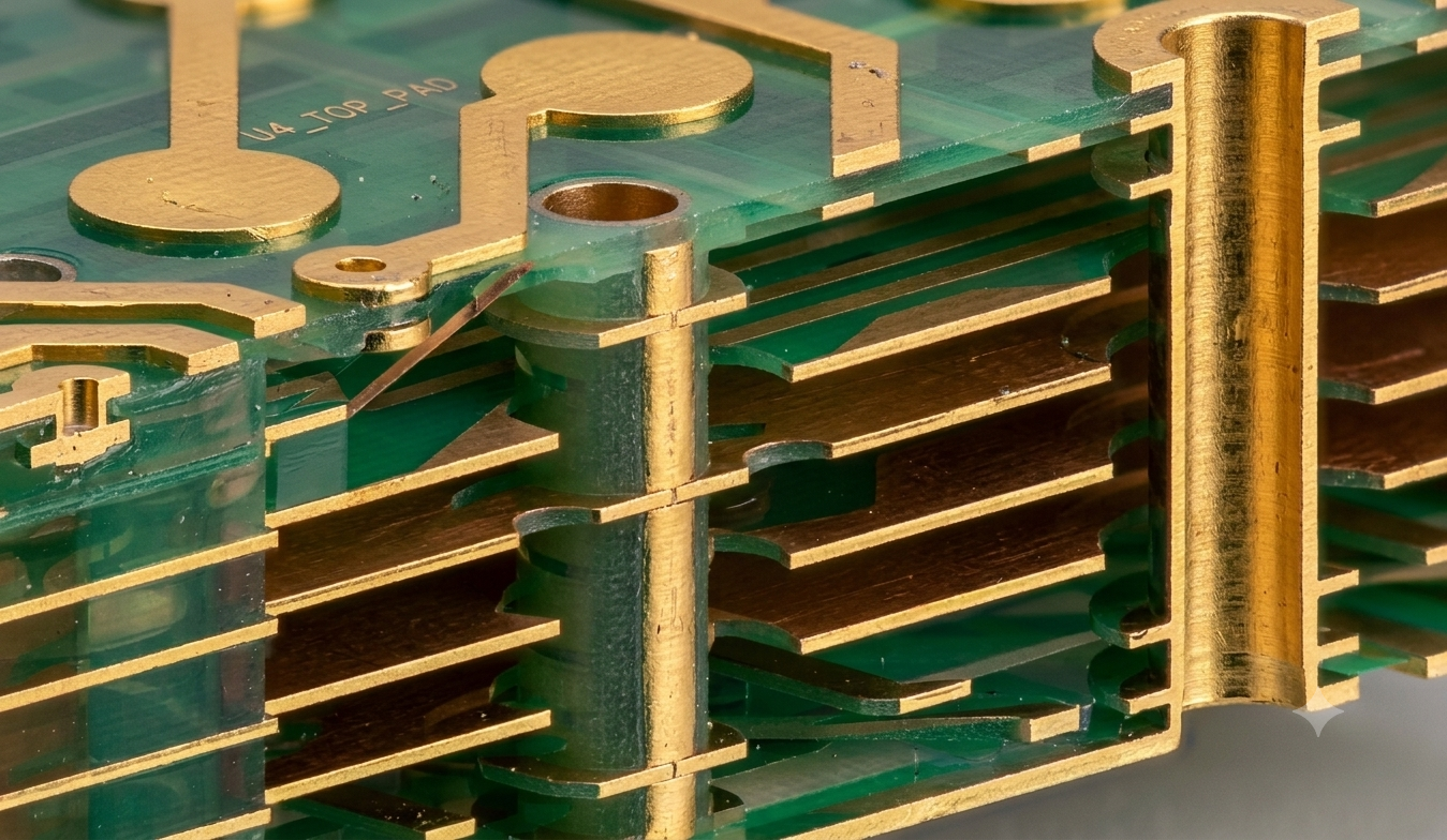
Multilayer PCB
Multilayer PCB
3D X-Ray inspection view
AOI inspection view
AOI inspection view
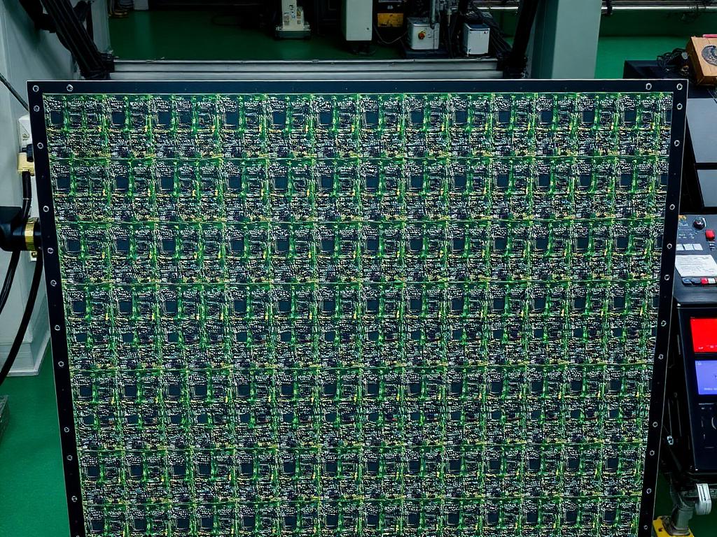
Production panel
Production panel

Illustrative process visuals — not customer-specific product photography.

FAQ

Frequently Asked Questions

Find quick answers to common questions about our Korean PCB manufacturing, DFM process, and global services.

Have a PCB or PCBA Project?

Send your files and get engineering feedback with a quote — DFM Review: 1–3 Business Days.

Detailed DFM feedback is provided after receiving sufficient manufacturing data.

Chat on WhatsApp